
In the connected world today, the demand to transfer data is growing every day. People increasingly consume streaming video content, at home and on the road. The increased bandwidth is needed on every level, from smartphones, PCs, at data centers and across long distance connections. This demand pushes the semiconductor industry to develop faster communication solutions for wireless, optical and wired interfaces.
For such high-speed communication interfaces chip designers need to limit the parasitic capacitance of the on-chip ESD protection clamps connected to the interfaces.
Traditional ESD approach for analog I/Os
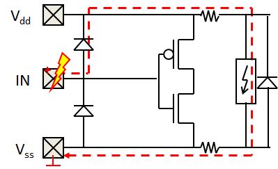
The traditional ESD approach for analog I/O pads is shown below in Figure 1. It consists of a diode from Vss to the I/O pad, a second diode from I/O pad to Vdd and a power/rail clamp between Vdd and Vss. IC designers like it because the 2 diodes are easy to implement, have a small silicon footprint and have reasonably low parasitic capacitance.
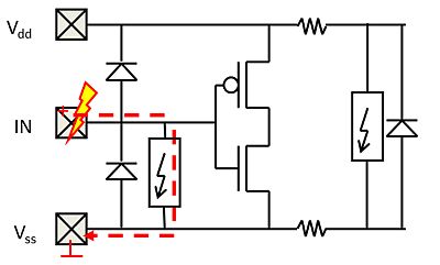
For sensitive nodes, IC designers add an isolation resistance from I/O to the circuit to increase the ESD design window. If the functional circuit cannot handle any ESD current, a secondary clamp is added behind the isolation resistance: Figure 2.

There are several issues with these simple ESD approaches, specifically for high speed interfaces:
- The isolation resistance severely impacts behaviour at high speeds and adds noise.
- The ESD diodes may introduce excessive parasitic capacitance between the signal pad and the power lines.
- Some interfaces cannot tolerate a diode from I/O pad to Vdd due to matching, due to noise coupling between pad and Vdd or because the signal voltage can be higher than the reference Vdd voltage.
- For sensitive nodes the total voltage drop over the intended ESD current path can be above the failure voltage of the functional circuit.
A simple way to reduce the capacitance (issue 2) and increase the voltage tolerance (issue 3) is to use 2 or more diodes in series. However, this leads to a higher voltage drop during ESD stress, deteriorating issue 4. An alternative with a novel dual bipolar concept [Link] was presented in 2017.
Local clamp ESD approach for analog I/Os
This article discusses an approach where IC designers replace the traditional dual diode ESD concept with a local protection clamp concept, simplified in Figure 3. If the functional operation cannot tolerate a diode from ‘IN’ to Vdd that diode can be removed. That is typical for fail-safe, Hot-swap, open-drain outputs, cold-spare inputs or overvoltage tolerant interfaces.
The local clamp approach introduces a lot of benefits:
- Reduced dependence on bus resistance
- Strongly reduced voltage drop under ESD conditions without the need for an isolation resistance, perfect for sensitive nodes.
- Different options to reduce the parasitic capacitance
- Can be optimized for each I/O pad separately. E.g. some pads may need higher ESD robustness or cannot tolerate a diode between I/O and Vdd.
More information?
Dual-diode based ESD protection is used a lot. However, some interfaces need another type of protection. A local ESD clamp in the IO area has many benefits. Sofics engineers have supported more than 100 fabless companies with customized local clamp solutions.
- Especially high-speed communication requires local clamps with low parasitic capacitance. You can get more technical details in peer-reviewed papers (2019, 2017, 2012) on our website.
- Some interfaces need higher voltage tolerance. In that case a diode to Vdd can be problematic. A local clamp concept can solve that. More information in our 2011 paper. [Link]
- Several applications (automotive, medical, consumer, HDMI, DisplayPort, USB, …) require much higher ESD robustness. Typically, most IOs are protected up to the standard 2kV HBM level. But interfaces that connect outside of the system need higher robustness. In 2009 an example solution for HDMI was presented [Link].
- Contact us if you like to discuss your application.


7 responses to “Local ESD protection in analog IOs”
[…] Interfaces that stay inside the package do not really need a complete I/O ring. A small I/O section close to the Through-Silicon Via (TSV) or pad/bump area can suffice. Of course, it is possible to reuse GPIO cells for such an IO section. But there is a great opportunity to reduce silicon area. It is recommended to use custom I/O and ESD cells. These can be smaller and can be designed with a different aspect ratio. It is also recommended to rely on local I/O protection clamps to reduce the need for nearby power protection clamps. More information on local ESD protection is available here (link). […]
LikeLike
[…] different strategy (see also our article about local ESD clamps – Link) is called for: local clamping to cut out the resistive path to and from the power […]
LikeLike
[…] transistors in advanced CMOS and FinFET processes. Several cases studies can be found here (link, link). The local clamp approach provides most flexibility to fine-tune the protection for each stress […]
LikeLike
[…] The technique has been verified on CMOS (40nm – 22nm) and FinFET (16nm – 5nm) processes and included in 30+ projects for high-speed interfaces like Ethernet. More information about this approach is available in earlier blog articles (link1, link2, link3) […]
LikeLike
[…] sensitive interface circuits. You can read more about it in several articles (link, link, link, link). The use of proprietary Silicon Controlled Rectifier (SCR) devices strongly reduced required area, […]
LikeLike
[…] localized protection can replace the traditional approach, reducing impact on performance and […]
LikeLike
[…] of the options for the ESD protection of the OVT driver is to use a local SCR-based clamp approach, in parallel to the driver circuit. The key advantages of this approach […]
LikeLike