
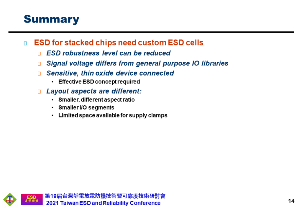
Semiconductor companies using 2.5D and 3D hybrid integration need to consider Electrostatic Discharge (ESD) protection early in the design, even for die-2-die interfaces that remain inside the package. There are several challenges but also opportunities. The use of a local ESD protection clamp at the TSV offers more robustness, higher performance, more flexibility, all in a strongly reduced silicon footprint.
The Sofics abstract was accepted for publication and presentation at the 2021 Taiwan ESD and Reliability conference. Due to covid19 travel restrictions the presentation was pre-recorded. The video is available below.
The slides can be browsed in the article below. The paper can be downloaded here.
Introduction
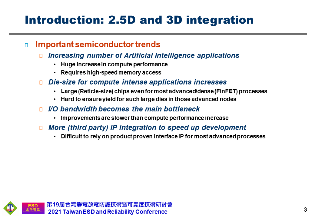
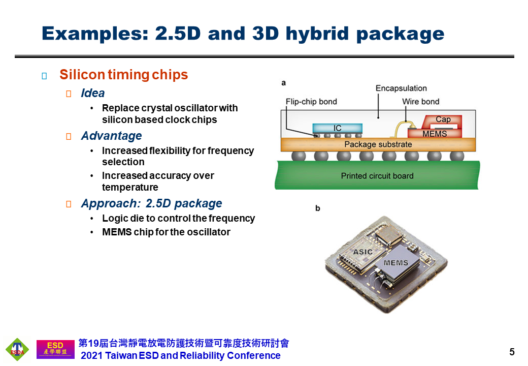
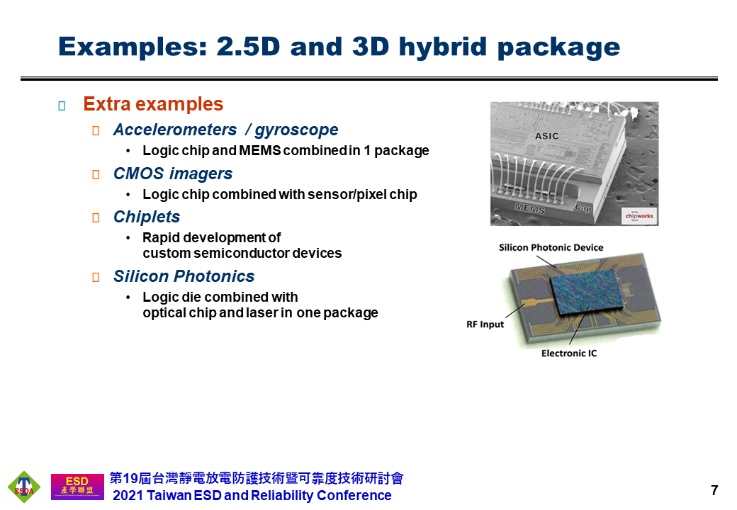
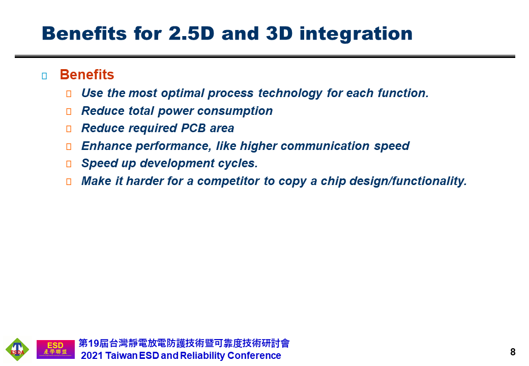
A growing number of semiconductor applications are turning to 2.5D and 3D integration for various reasons. Integrating multiple dies in a single package can provide several benefits.
- Reduce total power consumption
- Reduce PCB area and volume
- Enhance performance (e.g. faster compute to memory links)
- Speed up development cycles
- More robust against copying by competitors
- Select most optimcal process technology for each feature

ESD discussion
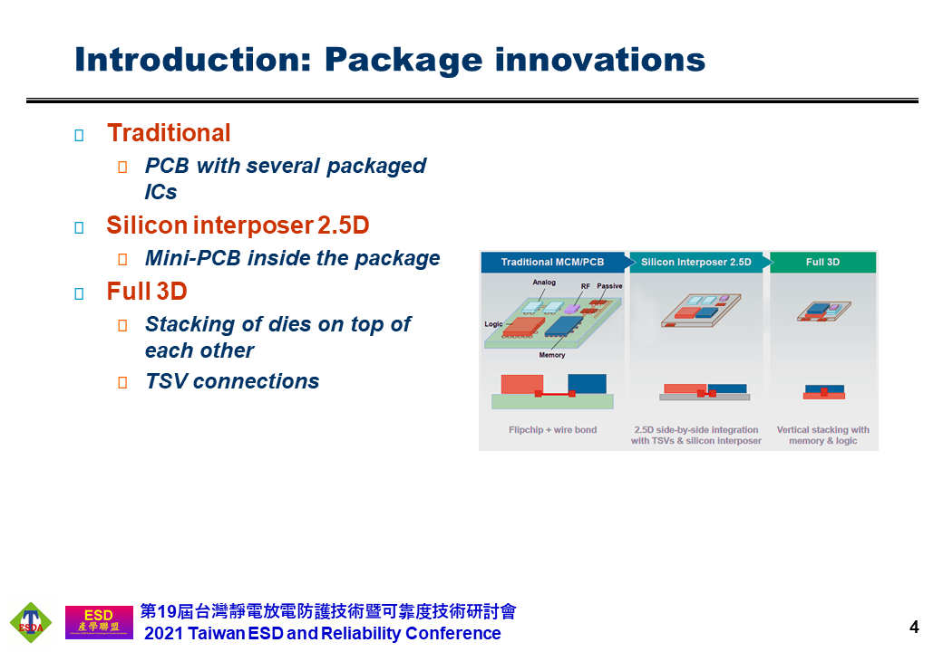
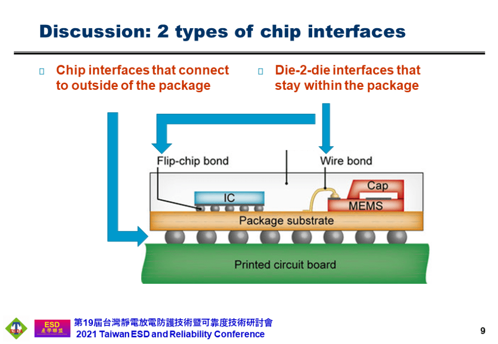
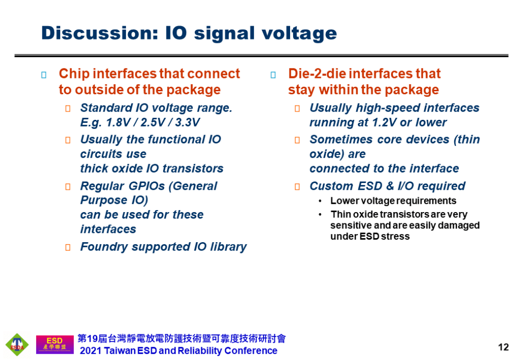
In 2.5D and 3D integrated packages there are 2 different interfaces.
- Interfaces that connect outside of the package
- Die-2-die interfaces that remain inside the package.
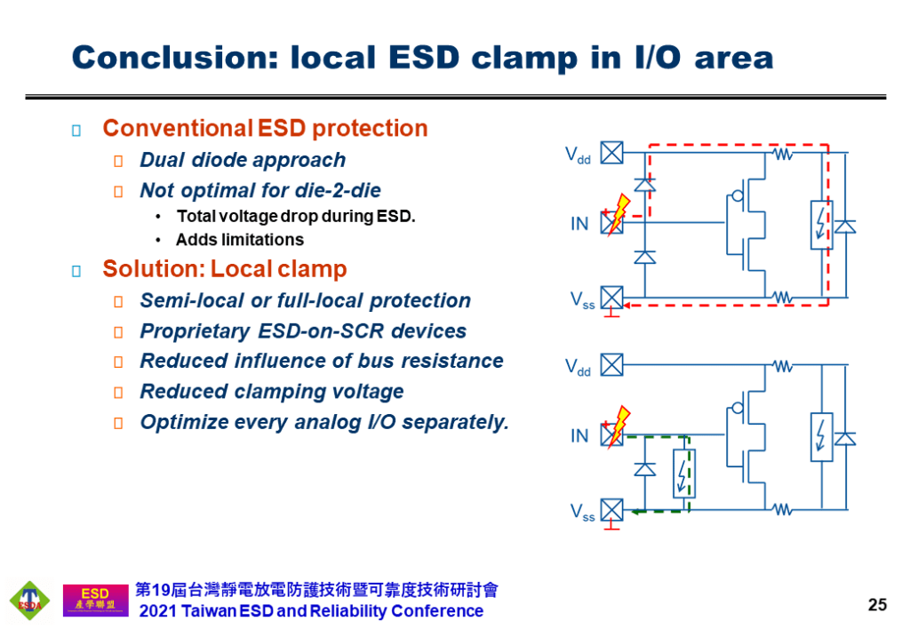
There is a clear difference between these 2 types for the relevant ESD requirement, the signal voltage and layout of I/O circuits and ESD devices. IC designers that use customized ESD cells can enjoy several benefits.

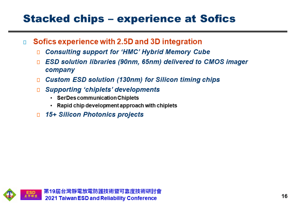
Sofics experience
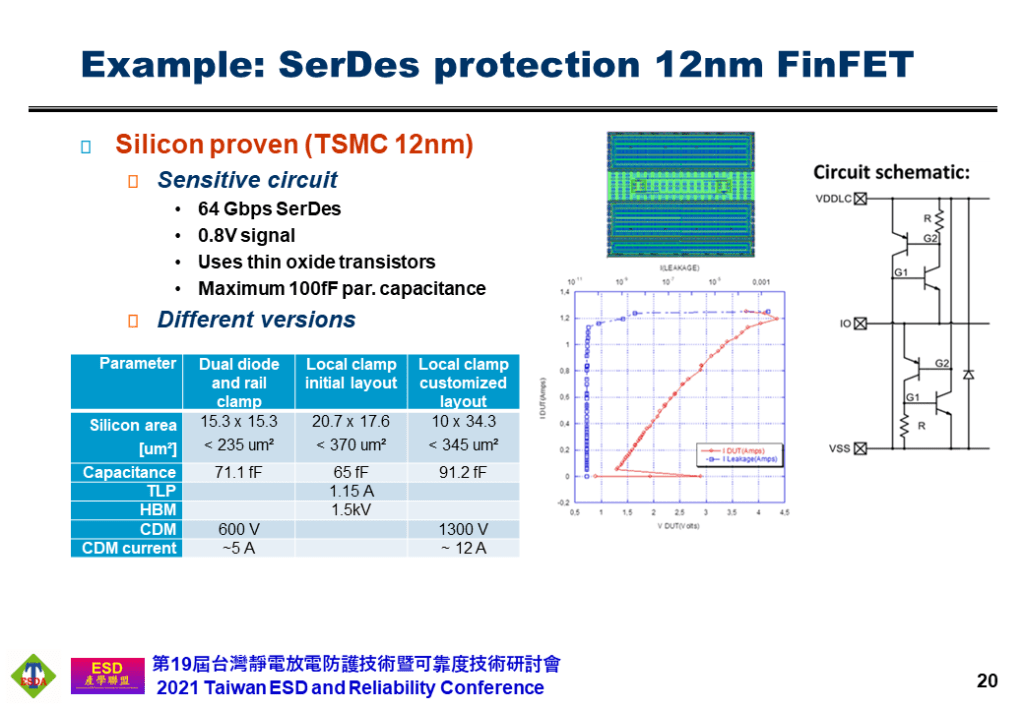
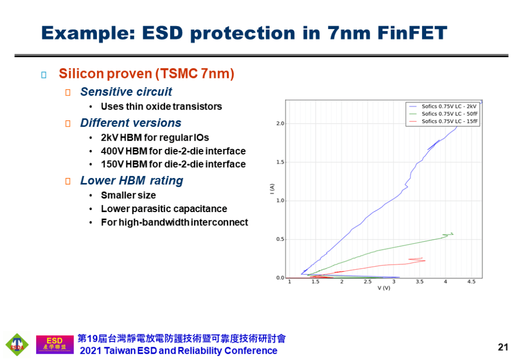
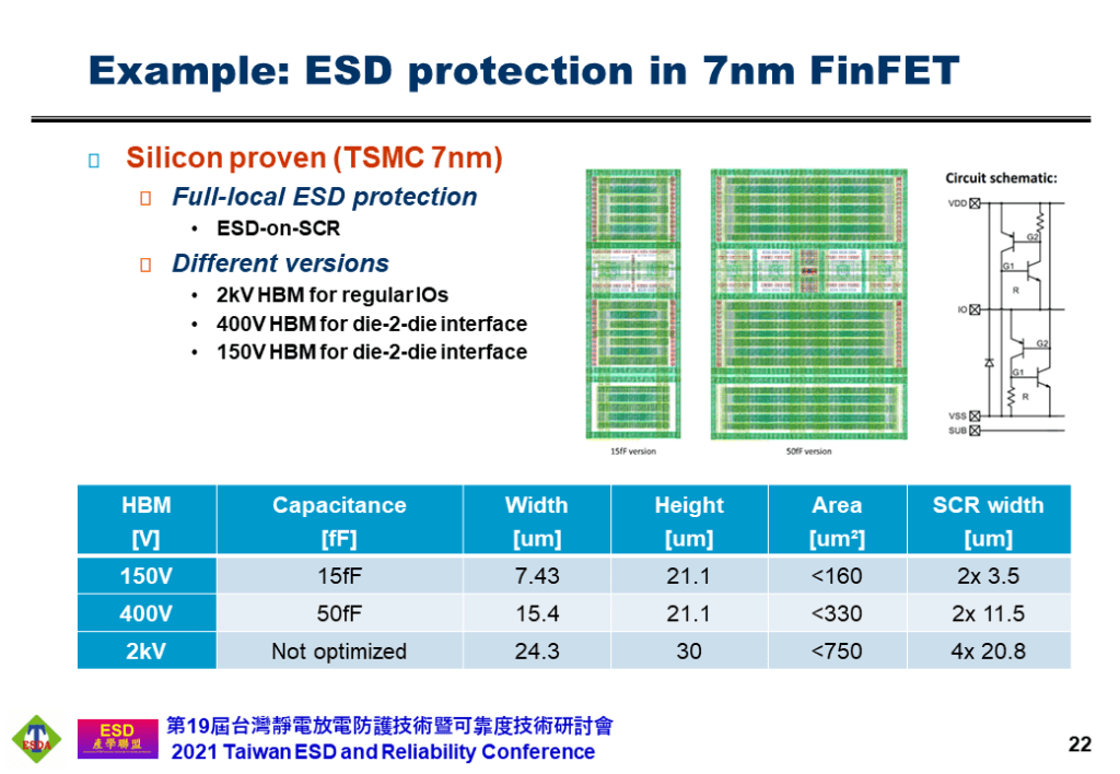
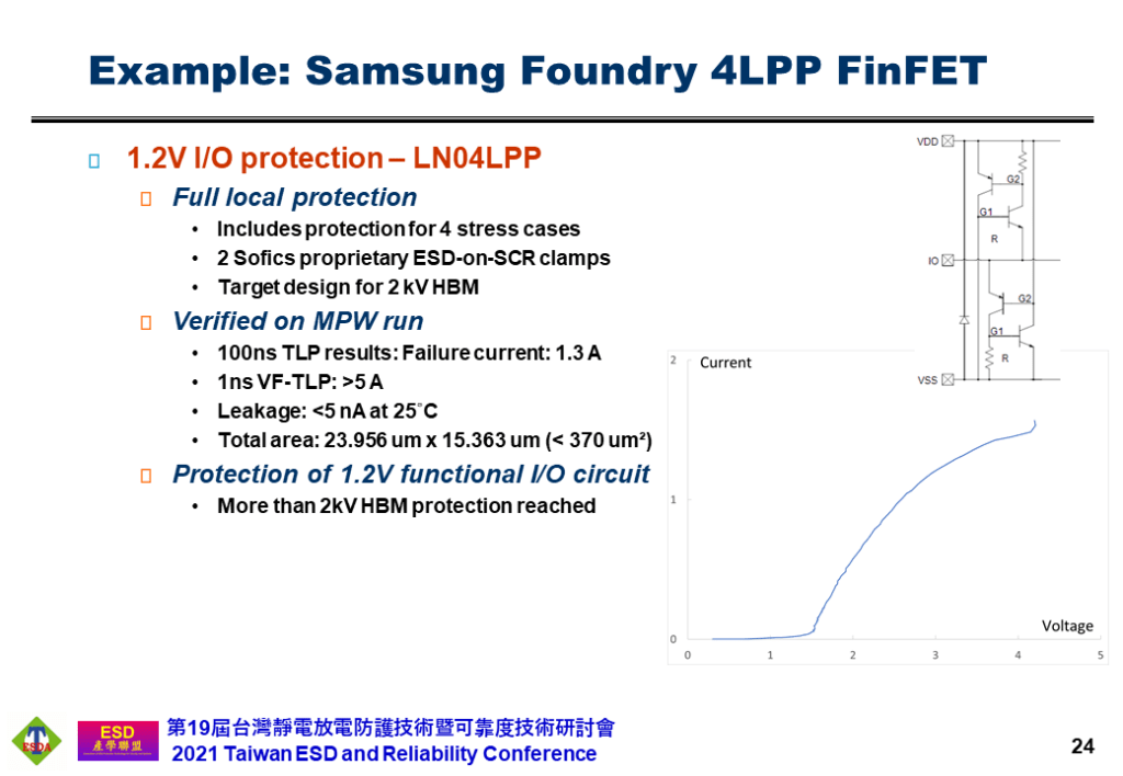
Sofics has supported a number of hybrid integration projects. The technology is easily adapted to match requirements. Several customers have used the local ESD protection clamps for their products. The presentation focused on low-cap ESD cells for high-speed die-2-die interfaces in FinFET technologies.


Awarded presentation!
The event was organized in a hybrid way. International presenters could not join in-person due to the travel restrictions in Taiwan. Fortunately, after the (recorded) presentation there was an opportunity to remotely discuss questions from the audience through a zoom call with the conference room. Plenty of relevant questions were discussed.
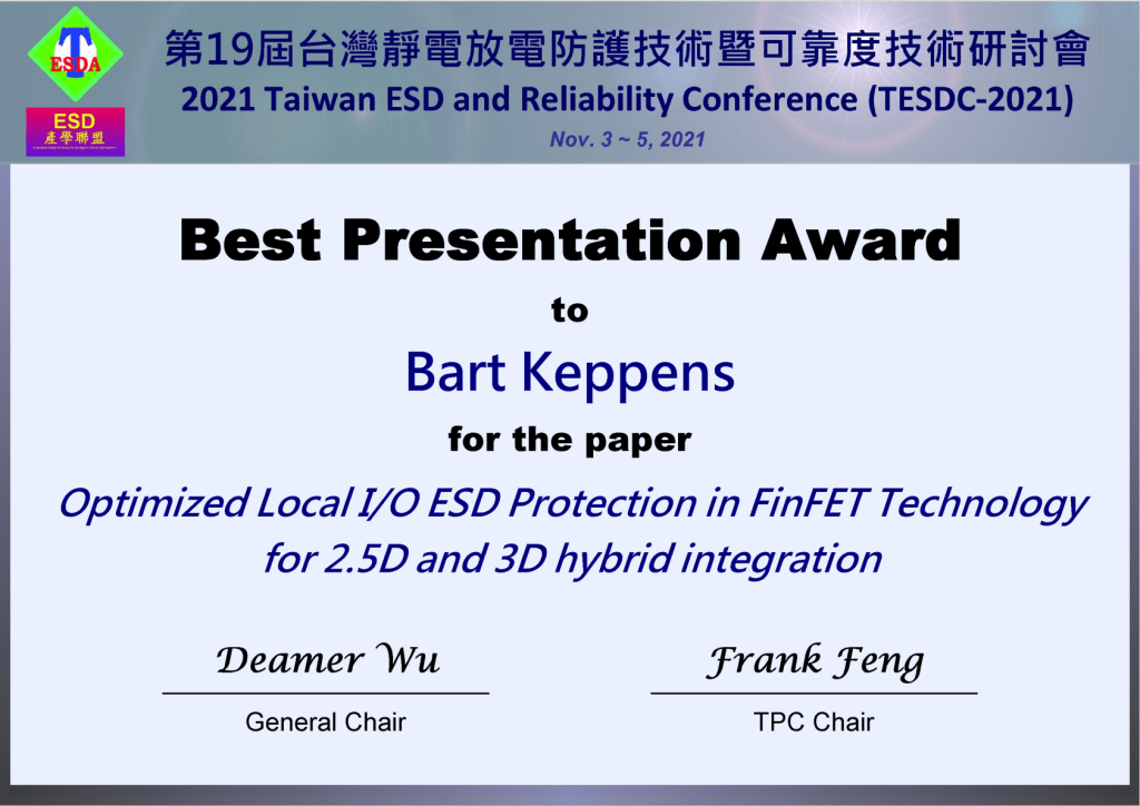
After the event the Sofics paper received the best presentation award.
Next articles…
Follow Sofics on LinkedIn, Facebook or Twitter to stay up-to-date about our next articles, tutorials and videos. Or subscribe by email below.


Leave a comment