
Paper published and presented at the 2024 Taiwan ESD and reliability conference
Ehsanollah Fallah, Bart Keppens
Sofics, 32 Sint-Godelievestraat, B-9880 Aalter, Belgium,
This paper is co-copyrighted by Sofics and the T-ESD Association
Sofics BV BTW BE 0472.687.037 RPR Oostende
Abstract: As semiconductor technology advances towards 3nm FinFet, mitigating electrostatic discharge (ESD) risks becomes increasingly vital. Integrating Chiplets introduces reliability concerns, particularly regarding ESD protection for various interfaces. This paper explores ESD mitigation strategies, focusing on internal interfaces crucial for Chiplet applications. Through simulations and measurements, the efficacy of an ESD-on-silicon-controlled rectifier (SCR), as a local clamp approach, is evaluated. Results demonstrate its superiority over conventional methods, offering ultra-low leakage and compact footprint. Furthermore, layout optimization techniques are discussed to minimize parasitic capacitance, essential for high-speed die-to-die interfaces.
Introduction
As Moore’s Law nears its end, scaling transistors for high-performance chips becomes tougher. Expanding chip area is crucial for enhancing performance, but it’s constrained by factors like cost, reticle size and manufacturing yield, leading to the emergence of the “area-wall”[1]. To jump from this wall, the semiconductor industry moved towards embracing Chiplet solutions across various applications. Chiplet solutions offer a promising alternative by exhibiting higher yields for equivalent chip areas, making them advantageous in overcoming the limitations of traditional monolithic chip designs[2]. Additionally, Chiplets enhances flexibility in selecting optimal processes for specific functionalities[3]. Moreover, Chiplet solutions boast reduced footprints while maintaining equivalent functionality compared to monolithic counterparts. Lastly, the reusability of Chiplets as Intellectual Property (IP) blocks promises to decrease overall design costs[4].
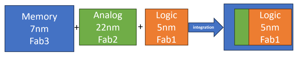
Fig. 1 illustrates the integration of a Chiplet solution. Various connectivity standards like UCIe[5], Bunch of Wires (BoW) [6], and Advanced Interface Bus (AIB) [5] have been introduced to facilitate communication between dies. Besides Chiplet advantages, designing a Chiplet-based solution has reliability challenges[7]. One of these challenges is providing effective Electrostatic Discharge (ESD) protection for different interfaces that Chiplets utilize for integration.
In discussions concerning ESD, it is crucial to categorize chip interfaces into two distinct types:
- External Chip Interfaces: These interfaces establish connections beyond the package boundaries, potentially utilizing methods like bond wires or ball/bumps.
- Internal Chip Interfaces: These interfaces are utilized within the package and employ various connection methods as mentioned before.
External interfaces are often integrated into an I/O-ring at the chip’s edge, utilizing various pad types provided by foundries. However, internal interfaces typically don’t require a complete I/O ring, with a small section near the Through-Silicon Via (TSV) sufficing.
On-chip ESD protection devices are crucial for mitigating ESD events on exposed package pins during various phases of the IC product lifecycle, including assembly, transportation, and testing. For the external interfaces, designers should adhere to standard ESD robustness criteria, usually requiring a minimum of 2kV Human Body Model (HBM) and around 300V to 500V Charged Device Model (CDM) protection. However, certain applications like HDMI cables, timing controllers, and SIM card interfaces may demand even higher ESD robustness exceeding 2kV HBM. Conversely, for chip interfaces contained within the package, the ESD robustness requirement can be adjusted. As these connections are sealed within the IC package, the risk of ESD stress during IC transport and PCB assembly is reduced. However, completely eliminating on-chip ESD devices is impractical, as ESD events could still potentially occur during the assembly of different dies inside the package. Nonetheless, such assembly processes are typically carried out under strict ESD-safe conditions, with assembly suppliers providing guidelines for minimum ESD requirements, usually less than 35V CDM[8].
The internal chip interfaces for Chiplet applications often require numerous connections, sometimes reaching several hundred. Each connection necessitates an ESD clamp, highlighting the need to minimize the area occupied by ESD cells. Additionally, many of these internal interfaces operate at high speeds, underscoring the importance of ESD solutions with minimal parasitic capacitance to meet these bandwidth demands effectively. In this paper, our attention is directed solely towards elucidating ESD solutions tailored specifically for Chiplet applications for 3nm and 4nm FinFET, wherein the imperative lies in implementing ultra-small ESD solutions characterized by minimal parasitic capacitance for these kinds of interfaces.
Traditional ESD approach vs SCR-based local clamp:
Fig. 2 illustrates the traditional ESD method, which includes two diodes at the I/O and a power clamp connecting VDD to VSS. While commonly used, this approach has limitations, including:
1. Sizeable Footprint.
2. Dependency on Bus Resistance: As the ESD discharge path inevitably incurs voltage drop attributable to bus resistance, the efficacy of this approach is contingent upon said resistance. Mitigation of this voltage drop mandates periodic replication of large power clamps at specific intervals.
3. Risk of Circuit Failure: Particularly for advanced nodes like 3nm or 4nm FinFet, the cumulative voltage drop along the designated ESD current path may surpass the failure voltage threshold of the functional circuit, posing a significant risk of circuit malfunction.;

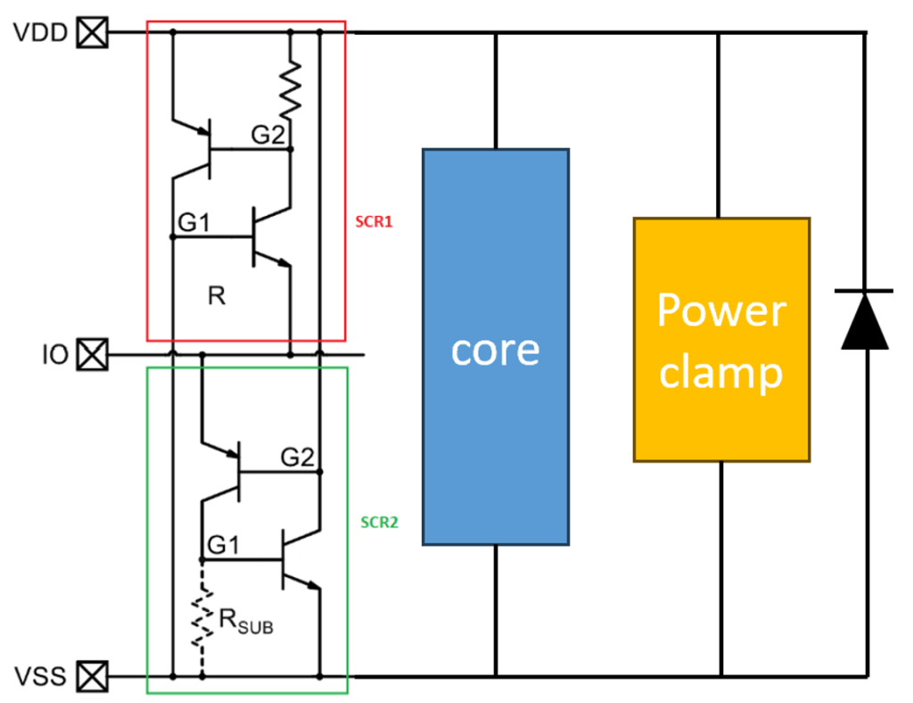
A full ESD local clamp solution can eliminate the mentioned issues. ESD-on-silicon-controlled rectifier (ESD-on-SCR) is a full local clamp approach comprising two SCRs. ESD-on can be customized easily to meet the ESD protection requirement for external and internal interfaces. Fig. 3 represents the ESD-on schematic. SCR2’s G2 node connects to VDD in this setup, while SCR2’s Anode connects to the IO pad. SCR2’s G1 connects to VSS through a well-resistor, while SCR1’s G1 connects directly to VSS, and its Anode and G2, via the well-resistor, are connected to VDD. This topology does not need any RC-triggering circuit, therefore it has lower leakage than RC-triggering clamps.
During standard operational conditions, the junction between the Anode of SCR2 and its G2 is reverse-biased, resulting in SCR2 being in a high-impedance state. Assuming the IO voltage never drops below the VSS threshold, SCR1 maintains its high-impedance state throughout normal operation, with its G1 connected to the ground and its cathode linked to the IO. ESD events occurring between the IO and VSS result in the VDD supply line entering a floating state. Initially, ESD current flows through the Anode-G2 junction, extending into the floating VDD bus and the interconnected circuits between VDD and VSS. Subsequently, as the current passes the Nwell diode from the IO to VDD, a rapid increase in VDD potential may activate the power clamp. A similar situation arises during ESD between VDD and IO, with the distinction that VSS becomes the floating node. Following the initial phase, SCR1 activates, providing a discharge path for the ESD current. During ESD between VSS and IO, the VDD remains floating while the IO exhibits a lower voltage relative to VSS. Consequently, the diode between the G1 of SCR1 and its cathode begins to activate, offering a discharge route for the ESD current. In scenarios involving ESD zap between VSS and VDD, an ESD diode from VSS to VDD facilitates the discharge path for ESD current. Conversely, to safeguard against ESD from VDD to VSS, various types of power clamps can be deployed. Options include RC-trigger or diode-trigger rail clamps[9], or alternatively, an RC-triggered SCR[10].
Performance evaluation
This section examines the performance of an ESD-on designed for external interfaces in 4nm technology by presenting the results of various measurements and simulations. The necessary layout adjustments to develop an ESD-on suitable for internal interfaces in Chiplet applications will be covered in the next section. Additionally, the modified ESD-on, as utilized in a Chiplet product, is introduced in the next section.
VFTLP performance
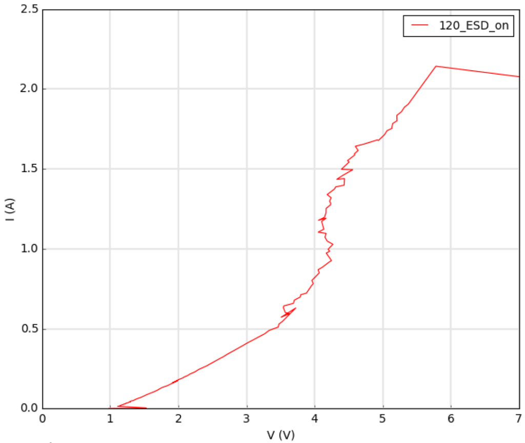
Given the established correlation between CDM and VFTLP pulses[11], the VFTLP machine is utilized to assess ESD-on performance under fast pulses. The VFTLP measurement results alongside the leakage measurement for ESD-on devices are depicted in Fig.3. VFTLP pulses, characterized by a 5ns width and 200ps rise time, are applied between the anode and cathode of SCR2 in Fig. 3. Due to the symmetrical topology of ESD-on, the same result is expected while measuring between the Anode and the cathode of SCR1. The designed device can accommodate a 5A VFTLP current. Depending on the package type, size and the correlation factor of the process, this 5A VFTLP can be translated to the CDM current. It is worth noting that this measurement has been performed on a stand-alone ESD-on structure on a bare die.
TLP performance
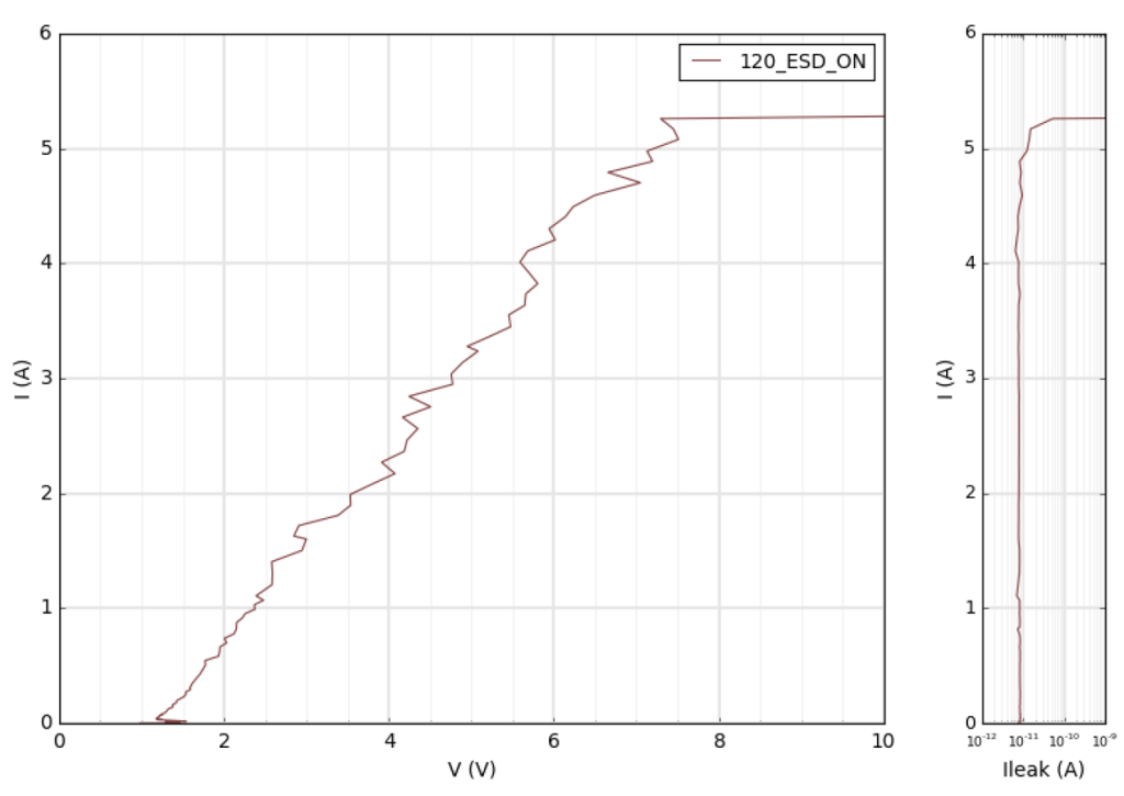
As previously mentioned, numerous external interfaces and IOs necessitate at least 2kV HBM. Leveraging the established correlation between TLP and HBM[11], the TLP tool assesses the ESD-on performance under HBM conditions. Fig. 5 presents the TLP measurement results for the designed ESD-on. TLP pulses, featuring a 100ns width and 10ns rise time, are applied between IO and VSS. Similarly, symmetrical topology ensures consistent measurement results when measuring between VDD and IO. This ESD-on device successfully withstands more than 2A TLP. It’s important to note that assessing holding and triggering voltages is best done through DC measurement.
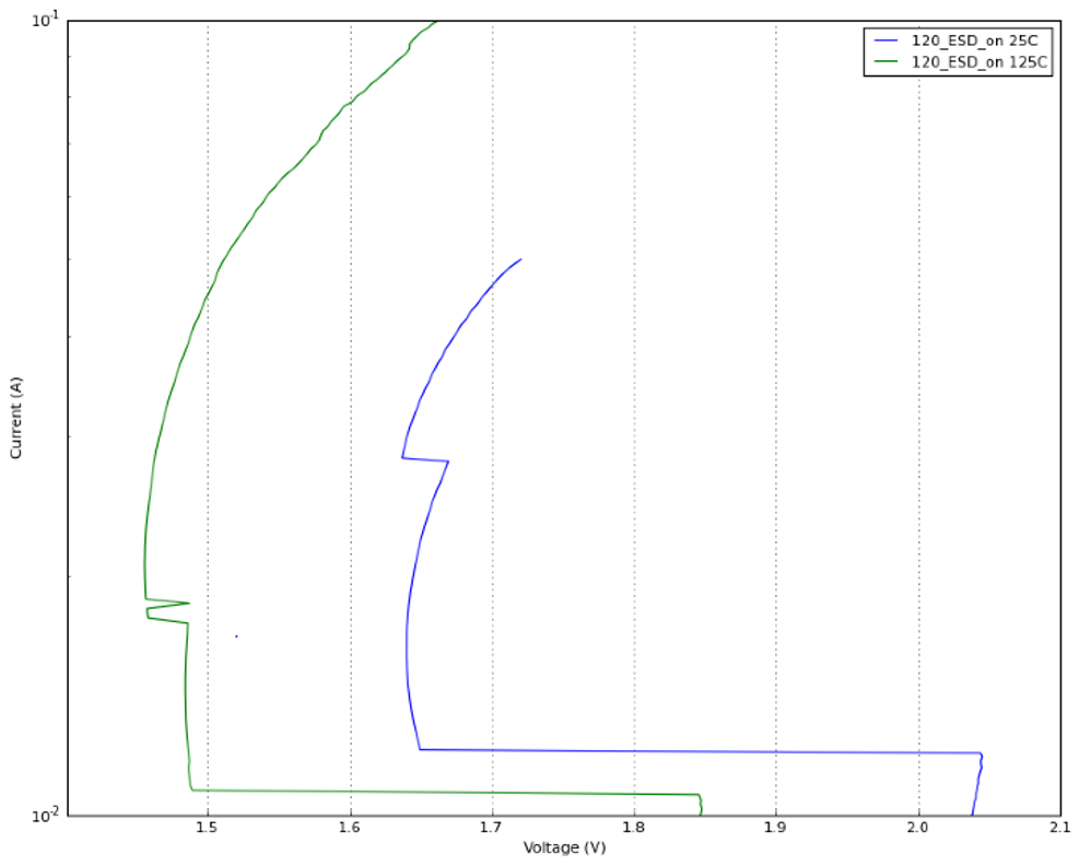
Holding and triggering
Ensuring latch-up immunity for any snap-back type ESD device necessitates a holding voltage exceeding the maximum VDD, typically 1.1 times VDD. Fig. 6 illustrates the DC measurement results for determining the holding voltage at both 25°C and 125°C. In this DC measurement, the current is swept between 0.001 and 0.1 A. The discussed ESD-on in 4nm is tailored for 1.2V IO, thus requiring a holding voltage exceeding 1.2V to ensure latch-up immunity. At 125°C, the worst-case scenario, the holding voltage measures 1.45V, confirming immunity against latch-up. Additionally, the triggering voltage must remain below the technology’s maximum handling capacity. At room temperature, the triggering voltage slightly exceeds 2V, falling within technology limitations.
Leakage performance
ESD-on operates without a triggering circuit, resulting in lower leakage compared to local clamps that require one. It’s intriguing to compare the leakage of ESD-on with other SCR-based ESD protections like RC-triggered SCR. Leakage measurements for ESD-on SCR and RC-SCR are depicted in Fig.7, conducted at both 25°C and 125°C. Both ESD-on and RC-SCR, designed for 1.2V IO, underwent leakage measurement through voltage sweep from 0V to 1.5V. ESD-on SCR exhibits sub-10pA leakage at room temperature, whereas RC-based triggered SCR shows ten times higher leakage under similar conditions.

Parasitic capacitance
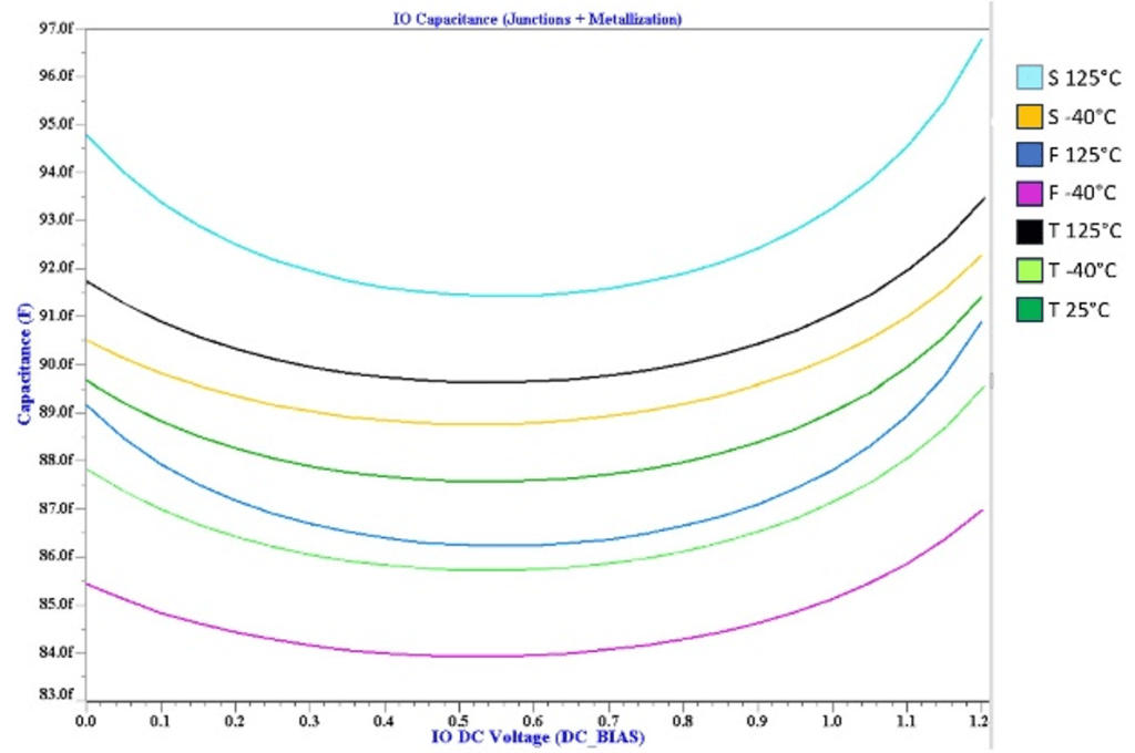
Parasitic capacitance simulations for three distinct corners (fast, slow, and typical) of ESD-on are depicted in Fig. 8. The horizontal axis represents total parasitic capacitance (the sum of junction cap plus metallization cap), while the vertical axis indicates voltage sweep over IO from 0 to 1.2V. Simulation encompassed all corners at -40°C and 125°C, with additional simulation conducted for the typical corner at 25°C. Results indicate that the total parasitic capacitance of ESD-on experiences less than a 7% variation across temperatures ranging from -40°C to 125°C for all corners compared to the typical corner at room temperature. Furthermore, within each corner, parasitic capacitance exhibits no more than a 7% deviation due to temperature fluctuations spanning from -40°C to 125°C.
Customized ESD-on for Chiplet applications
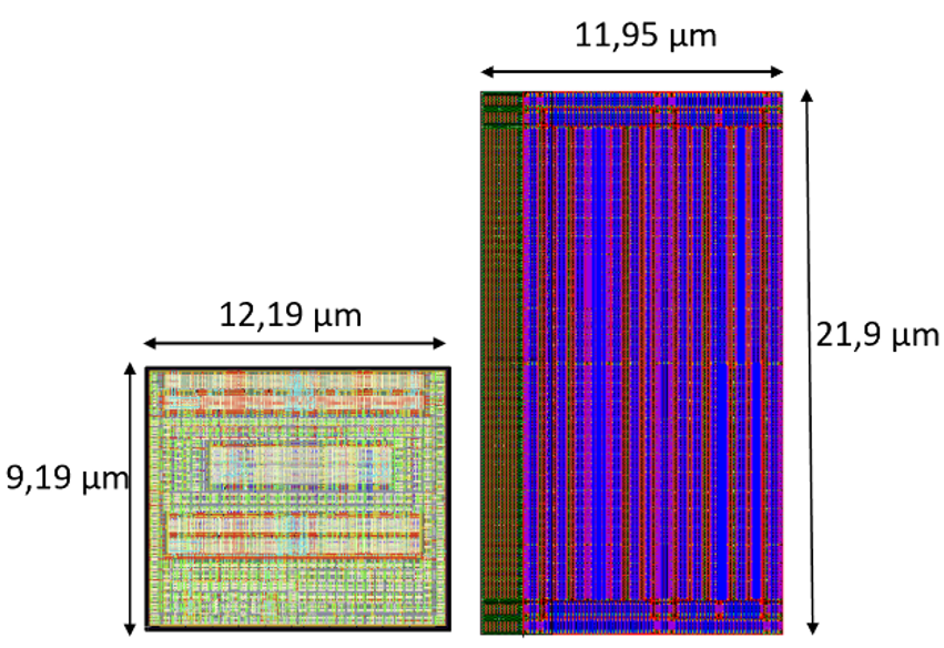
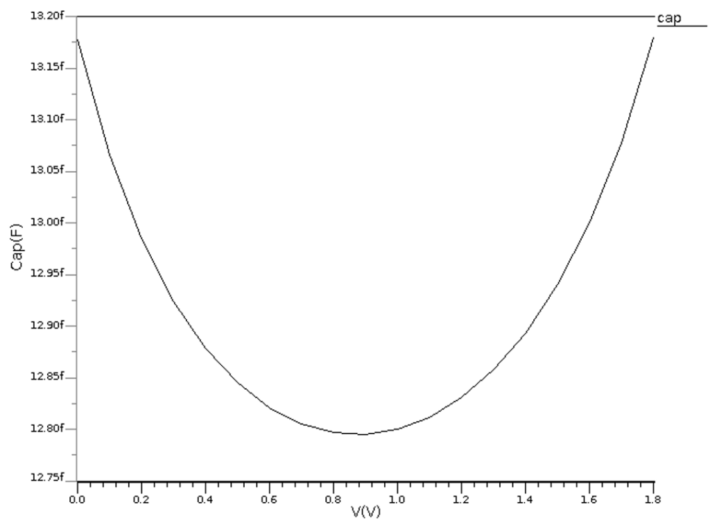
The designed ESD-on in 4nm, with the parasitic capacitance of 91fF for the typical corner at room temperature, can effectively withstand 5A VFTLP. However, this capacitance level may not be suitable for numerous high-speed interfaces in 2.5D/3D applications. Fortunately, such interfaces are typically not exposed to 5A VFTLP. The Industry Council recommends a protection level ranging from 30V to 5V CDM for these interfaces[8]. Thus, a smaller clamp tailored for internal interfaces of Chiplet applications can be employed, resulting in reduced total parasitic capacitance. Fig. 9 illustrates a comparison between two ESD-on layouts, with the smaller variant designed for 1A VFTLP. This compact ESD-on has been integrated into a Chiplet product for AI applications. To evaluate its performance, VFTLP pulses with 5ns width and rise time of 200ps are applied between different for different combinations. To prevent product damage, measurements were halted at the targeted 1A level. The result of these measurements can be found in Fig.10. Fig. 11 represents the result of parasitic capacitance simulations for the typical corner at room temperature. The maximum tolerated parasitic capacitance for the internal interfaces of this Chiplet product is less than 15fF. The tailored ESD-on with parasitic capacitance below 13.2 for the typical corner at room temperature successfully met this requirement. In the next section, the different steps that are followed for this layout customization are presented.

Layout considerations for the high-speed die-to-die interface
Reducing the total parasitic capacitance is the goal of this optimization. The total parasitic capacitance at the I/O pad is multifaceted, incorporating junction capacitance derived from foundry-supplied Spice models for diodes. Additionally, metal connections to local ESD clamps contribute significantly, with parasitic metal capacitance determined through PEX extraction. For advanced Finfet nodes, more than 60 % of the total parasitic cap is because of metalization. Table 1 shows this fact for ESD-ons in 3nm FinFet for different IO voltages. It is worth mentioning that these devices are not customized for die-to-die applications. While reducing metal width reduces capacitance, it compromises connection robustness. Therefore, the minimum width of metal lines depends on the amount of maximum ESD current that passes through them. This minimum width can be derived from the design rule manual of foundry. Metal dummies in PEX extraction are also added as a part of metalization. For high frequencies (>50 GHz), parasitic capacitance acts as a ground resistance, necessitating sufficient impedance. A 15 fF capacitance translates to ~200 ohms resistance at 50 GHz.

In the iterative process to mitigate parasitic capacitance from metal connections, several rules are applied:.
- Reducing parasitic metal capacitance for IOs involves positioning the IO lines as distant as possible from VDD and VSS lines.
- Metal dummy usage significantly impacts metalization parasitic capacitance. Often, dummy metal generation lacks optimization for minimal capacitance, allowing for the removal of excess dummies without density violations.
- Junction capacitance reduction is limited unless it compromises ESD performance, typically constrained to 30V CDM[8] for die-to-die interfaces in standard-sized packages.
- Unnecessary connections should be removed to mitigate parasitic effects.
- Minimizing Metal 1 presence to connected diffusion, avoiding Metal 1 crossing junctions, and favoring vertical connections are strategies to reduce parasitic effects.
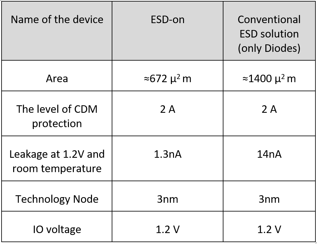
ESD-on versus traditional ESD approach in 3nm
Table 2 presents a comparative analysis of ESD-on as a local clamp solution versus conventional ESD methods in the context of 3nm technology. ESD-on demonstrates remarkable size reduction, exceeding 100% in comparison to the Dual-diode approach. Notably, besides its compactness, the dual diode method necessitates the repetition of power clamps at fixed intervals, contributing to significant space consumption. For instance, a typical rail clamp in conventional ESD solutions occupies approximately 1237 µm². Conversely, the local clamp approach minimizes the need for frequent repetition of such large power clamps, resulting in substantial area savings. Additionally, ESD-on exhibits tenfold lower leakage compared to traditional ESD solutions at room temperature.
Conclusions
Traditional ESD methods face limitations in size, reliance on bus resistance, and circuit failure risks, especially in advanced nodes. The ESD-on-silicon-controlled rectifier (SCR) emerges as a compact, customizable solution with lower leakage. Evaluation of ESD-on SCR performance for 4nm and 3nm technologies reveals efficacy in meeting stringent ESD requirements while minimizing footprint and maintaining high-speed operation. Customization for internal Chiplet interfaces emphasizes minimizing parasitic capacitance. Layout optimization strategies focus on reducing metal capacitance and optimizing metal dummy usage. Comparative analysis shows ESD-on’s advantages over traditional methods, including smaller footprint, comparable or superior ESD protection, and lower leakage. In essence, ESD-on SCR represents a significant advancement in addressing ESD challenges in Chiplet-based designs, ensuring reliability and robustness in future semiconductor products.
Important: As is the case with many published ESD design solutions, the techniques and protection solutions described in this paper are covered under patents and cannot be copied freely.
References
[1] Han, Yinhe & Xu, Haobo & Lu, Meixuan & Wang, Haoran & Huang, Junpei & Wang, Ying & Wang, Yujie & Min, Feng & Liu, Qi & Liu, Ming & Sun, Ninghui. (2023). The Big Chip: Challenge, Model and Architecture. Fundamental Research. 10.1016/j.fmre.2023.10.020.
[2] Li, Tao & Hou, Jie & Yan, Jinli & Liu, Rulin & Yang, Hui & Sun, Zhigang. (2020). Chiplet Heterogeneous Integration Technology—Status and Challenges. Electronics. 9. 670. 10.3390/electronics9040670.
[3] Gujar, Vivek. (2024). Chiplet Technology: Revolutionizing Semiconductor Design-A Review. Saudi Journal of Engineering and Technology. 9. 69-74. 10.36348/sjet.2024.v09i02.006.
[4] Kim, Jinwoo & Lee, M. & Torun, Hakki & Roy, Kallol & Swaminathan, Madhavan & Mukhopadhyay, Saibal & Krishna, Tushar & Lim, Sung & Murali, Gauthaman & Park, Heechun & Qin, Eric & Kwon, Hyoukjun & Chaitanya, Venkata & Chekuri, Venkata Chaitanya Krishna & Dasari, Nihar & Singh, Arvind. (2019). Architecture, Chip, and Package Co-design Flow for 2.5D IC Design Enabling Heterogeneous IP Reuse. 1-6. 10.1145/3316781.3317775.
[5] Yang, Zhuoping & Ji, Shixin & Chen, Xingzhen & Zhuang, Jinming & Zhang, Weifeng & Jani, Dharmesh & Zhou, Peipei. (2024). Challenges and Opportunities to Enable Large-Scale Computing via Heterogeneous Chiplets. 765-770. 10.1109/ASP-DAC58780.2024.10473961.
[6] Farjadrad, Ramin & Kuemerle, Mark & Vinnakota, Bapiraju. (2019). A Bunch of Wires (BoW) Interface for Inter-Chiplet Communication. IEEE Micro. PP. 1-1. 10.1109/MM.2019.2950352.
[7] Rupe, Jason. (2024). Reliability and Chiplets. IEEE Reliability Magazine. PP. 1-1. 10.1109/MRL.2024.3386643.
[8] “Industry Council on ESD Target Levels White Paper 2: A Case for Lowering Component- level CDM ESD Specifications and Requirements Part II: Die-to-Die Interfaces Industry Council on ESD Target Levels August 2023 Revision 1.0.” Available: https://esdindustrycouncil.org/ic/en/shared/industry-council-white-paper-2-pii-rev-1.0-final.pdf
[9] Tang, Hongju & Cai, Xiaowu & Liu, Xinghui & Liu, Hainan & Luo, Jiajun & ZHAO, Haitao & Peng, Rui & Xu, Dongsheng. (2018). Design of Power Clamp Circuit with Diode String and Feedback Enhanced Triggering in advanced SOI BCD Process. 1-3. 10.1109/ICSICT.2018.8565711.
[10] Li, Nanjin & Han, Aoran & Xiaozong, Huang & Chen, Le & Zhang, Yuxin & Li, Jieling & Liu, Yi & Liu, Jizhi & Liu, Zhiwei. (2022). RC-Coupled SCR devices for advanced nanoscale COMS process. 1-3. 10.1109/ICSICT55466.2022.9963253.
[11] Zhou, Yuanzhong & Hajjar, J.-J. (2008). CDM ESD failure modes and VFTLP testing for protection evaluation. International Conference on Solid-State and Integrated Circuits Technology Proceedings, ICSICT. 333 – 336. 10.1109/ICSICT.2008.473453..
