
A typical overvoltage tolerant (OVT) driver is a stack of two devices. The first device connected to rail is used to switch the I/O voltage, while the second device connected to pad is used to protect against the high voltage.
In this article, we will have a look at a couple of possible SOA (safe operating area) issues that arise from this commonly used topology. We will do this with a concrete case study: the NMOS part of a 1.8V driver making use of 0.9V devices (Vmax = 1V). A fully analogous story for the PMOS driver is possible too.
DC SOA issue
First we will take a look at the distribution of the voltages if the NMOS driver is off and the pad is driven high. The bottom switching MOS is turned off, and the gate of the protection MOS is placed at a midrail voltage of 0.9V.
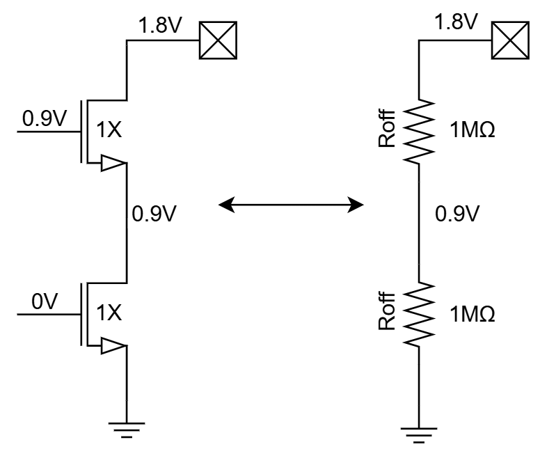
The first case we will look at is if both devices have equal sizing.
To estimate what DC voltage will exist at the midnode, we take a look at the off resistance of both MOS devices. If we assume the midnode to be at 0.9V, both MOS devices have identical voltages across their terminals, and will thus have an equal off resistance. Indeed, the pad voltage will distribute itself evenly across both devices and our initial assumption of 0.9V is confirmed.
However, our initial assumption of both off resistances being identical is not always true. This could have various reasons. For example, the sizing of both devices could be different. Another reason could be the difference in bulk voltage or isolation of both devices, leading to different leakage currents. These are just a few reasons from a whole laundry list why they could be different that could lead to a DC SOA issue. Careful design and simulation is required to verify if the DC behavior is good.
Transient SOA in falling edge
DC is not the only time we have SOA issues. They are also seen in every transition. In this section, we will focus on the falling edge of the transition.
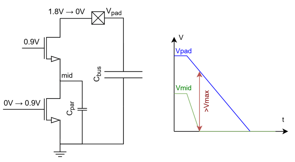
If we look at the voltage waveform, we can clearly see the drain-source voltage of the switching MOS go above Vmax, leading to a SOA violation. Vpad falls more slowly because of two reasons.
First of all, the capacitive load seen by the pad and the midnode is significantly different. The pad sees the full bus capacitance, while the midnode only sees the parasitic capacitance of both driver MOS devices. The bus capacitance is often orders of magnitude larger than the parasitic capacitance seen at the midnode. Due to this difference in capacitive load, it is evident the midnode voltage will fall much faster than the pad node.
A second reason why the midnode falls much faster is because the gate-source voltage of the switching and protection MOS are significantly different. The switching MOS is driven by the full 0.9V swing, so its conductivity is maximal. On the other hand, the gate-source voltage of the protection MOS is (0.9V-Vmid). During transition this voltage is significantly lower, so the conductivity of the protection MOS will be lower as well. In other words, Vmid is pulled down very strongly by the switching MOS while Vpad is pulled down more weakly by the protection MOS.
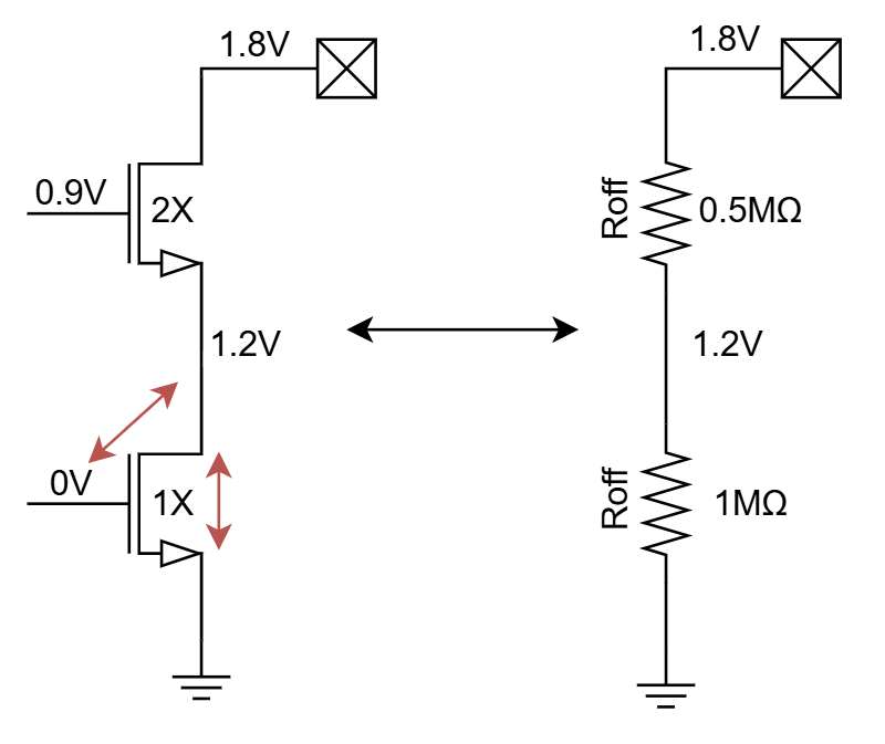
The most straightforward solution is to increase the size of the protection device. This however creates the DC SOA issue discussed earlier, and will also increase the SOA issues during the rising edge. On top of that, it will increases the size and leakage of our driver.
Transient SOA in rising edge
We have a SOA issue in DC, we have a SOA issue in the falling edge of the path, so of course we also have one in the rising edge of the pad!
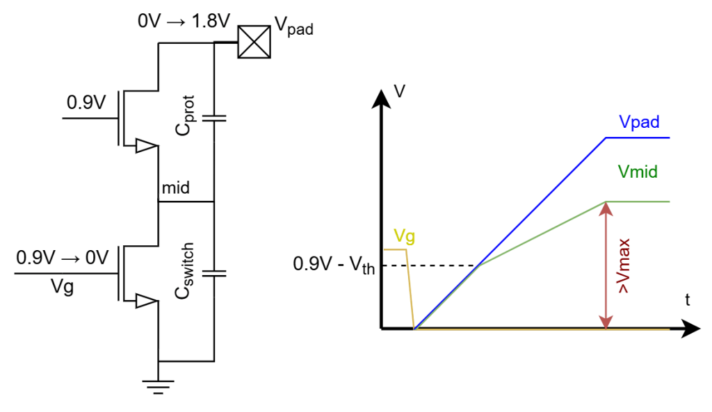
To see where this higher voltage comes from, it is easiest to look at what happens on the mid node. Initially the voltage is zero, and we have a strong connection to the pad through the protection MOS which is conducting well. So Vmid follows Vpad closely. However, when Vmid starts rising, the gate-source voltage of the protection MOS drops. When Vmid reaches a threshold below 0.9V, the protection MOS stops conducting and the mid node becomes high impedant. In this example, the threshold voltage is 0.3V so the mid node becomes high impedant once it reaches 0.6V .
Now it is controlled by the lowest impedant element in our circuit, which are the parasitic drain to source capacitances of the driver MOS. If we assume both MOS to be equal, we can assume their parasitic capacitance is also roughly equal. We now have a half capacitance divider from pad to mid node. So for every volt the pad rises, the midnode rises by half a volt. In our example, this is the pad rising from 0.6V to 1.8V, leading to an increase in Vmid of 0.6V. In other words, the Vmid at the end becomes > Vmax!
This is assuming both MOS have an equal drain to source capacitance. A possible solution would thus be to increase the size of the switching device compared to the protection device, increasing its parasitic capacitance and thus lowering the amount Vmid will go up once it is high impedant. For the falling edge however, we proposed to increase the size of the protection MOS compared to the switching MOS: the exact opposite of what we want to do now…
Conclusion
The most typical design of an overvoltage driver is a stack of two MOS devices, where the second device is used to limit the voltage over the bottom device and the first device is used to switch the pad voltage. A case study was done for this topology for a 1.8V NMOS driver using 0.9V devices. SOA violations were seen in DC and both rising as well as falling pad transitions. Solving these issues by changing the driver size is not possible, since falling and rising edge have conflicting size requirements. In other words, even though in theory the standard stacked driver should work for this use case, in practice it does not.
At Sofics we solve these issues by making use of additional control circuitry and different stacking architectures, enabling us to stay within SOA limits while still enabling higher voltage ratings.

4 responses to “Typical SOA violations in a stacked driver”
[…] allowable signal swing of the input signal for these standard input circuits is determined by the Safe Operating Area (SOA) of the transistors used. Such a circuit implemented with transistors having an SOA of 3.3V […]
LikeLike
[…] Typical SOA violations in a stacked driver – link […]
LikeLike
[…] is available in a set of articles (I/O specs explained, Types of overvoltage tolerant I/O, Typical SOA violations in a stacked driver, overvoltage tolerant receiver […]
LikeLike
[…] The IO voltage of 1.8V + 10% stays below two times the maximum tolerance of the devices. This means it is possible to use a stack of two devices when the intermediate voltage is well controlled. Just stacking 2 transistors is not enough. Both during DC and transients there could be Safe Operating Area (SOA) violations. More information about SOA issues in our earlier article. […]
LikeLike