
In general, the input section of a digital I/O can be a relatively simple circuit, such as an inverter. Furthermore, these circuits exhibit excellent performance regarding input impedance (which is exceptionally high), power consumption (negligible under steady-state conditions), and speed (extremely fast).
Under certain conditions, it is necessary that an input section is OverVoltage Tolerant (OVT). For example designing a 5V legacy input with a 3.3V technology limit, or designing an input with only core transistors for reasons of speed or radiation hardness.
This additional requirement will often lead to a new trade-off, where concessions will have to be made in terms of speed, input impedance, power consumption or circuit complexity.
Typical receiver architectures
In non-OVT applications, a typical digital input circuit consists of a CMOS Schmitt trigger circuit, as illustrated below.
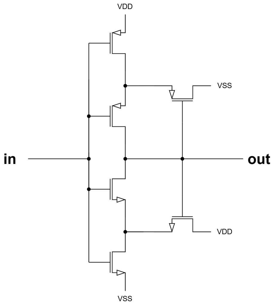
The main benefits of this circuit are:
- Hysteresis: in order to filter out input noise or ringing
- High input impedance: Only mosfet gates are connected to the input
- Low static power consumption: No currents are flowing when the circuit is not switching
- Speed: the input capacitive load can be low
An alternative solution involves employing an input differential pair, suitable for handling both differential and single-ended signals. When used for single-ended signaling, one input terminal is tied to a reference voltage. This method offers several advantages, including improved dynamic range, signal integrity, and reduced distortion. With certain modifications, hysteresis can also be incorporated. However, the primary disadvantage compared to a simple inverter or Schmitt trigger input circuit is the constant power consumption, even when the circuit is not switching.
OVT
The allowable signal swing of the input signal for these standard input circuits is determined by the Safe Operating Area (SOA) of the transistors used. Such a circuit implemented with transistors having an SOA of 3.3V can only handle input signals below 3.3V. Applying a 5V swing signal at the input will likely result in damage. In the case of a Schmitt trigger, for instance, this would create an electrical overstress condition between the gate and source of the lowest nmos transistor.
Voltage division
The most straightforward way to make an input circuit overvoltage tolerant is to add a voltage divider circuit as shown below:
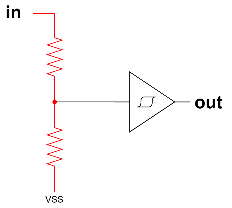
This approach has the benefit of its simplicity. Moreover, by choosing the appropriate resistor ratios, almost any input voltage range can be obtained. Nevertheless, there are some important drawbacks as well:
The main drawback is that the high input impedance property is nullified. When a pull-up or pull-down resistor is already present, this may not be a significant issue. However, in many cases, a pull-up/down resistor is absent or can be disabled, and adding the voltage divider results in a substantial reduction of the input impedance from the >TΩ-range to the kΩ or MΩ range.
A second drawback is the loss of bandwidth. The resistance of the voltage divider (which is typically chosen as high as possible to obtain an as high as possible input impedance), together with the input capacitance of the non-OVT input circuit forms a low pass filter. As a result, the reaction speed of the OVT-input circuit is reduced.
Next to the two most common drawbacks mentioned above, the voltage divider circuit can also negatively influence other specifications such as the noise and sensitivity.
Clipping
Next to voltage division at the input, also voltage clipping can be a valuable alternative for increasing the allowable input voltage range.
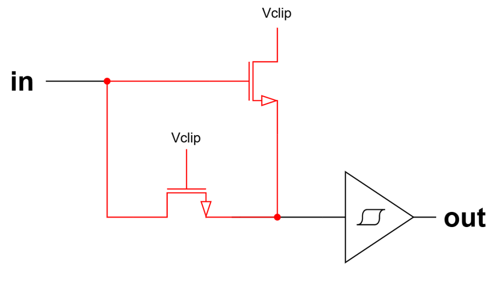
The circuit illustrated above will pass all input signal levels below ‘Vclip’ and block voltages beyond ‘Vclip’ replacing them by ‘Vclip’. This is a valid approach as long as the switching levels for the entire input circuit are specified below ‘Vclip’.
This approach might lead to a minor loss of input impedance, but most of the drawbacks of the voltage divider are not present here. There is no static power consumption, no low pass filter behaviour…
Pay attention that the maximum voltage difference between the input signal and Vclip is limited by the SOA of the transistors used by the clipping circuit. As a result, using transistors with an SOA-limit of Vmax, the final input swing cannot be extended beyond 2Vmax.
More advanced solutions
Using voltage division or clipping, already a fair spectrum of OVT input applications can be covered, whereby some concessions will need to be made. Beyond these limitations, Sofics has developed its proprietary portfolio of OVT input circuits which circumvent these concessions and allow the design of e.g. an OVT input circuit with high input impedance (>TΩ-range), at high speed, without static current consumption and switching levels over the full input swing range.

3 responses to “Overvoltage tolerant receiver structures”
[…] The ‘Overvoltage tolerant’ requirement basically means that an I/O that normally runs at 3.3V for instance (driving, receiving at 3.3V) must be able to withstand higher voltage transients like 5V. Some people refer to this as input overvoltage tolerance. During operation the I/O voltage can be higher than the supply voltage. This affects the design of the I/O circuit because without consideration of these higher voltages it can damage the circuit. It also affects the ESD protection approach. A (parasitic) diode between I/O and Vdd will allow current to flow from a 5V signal to the 3.3V supply line, pushing the 3.3V supply to a higher voltage. Our colleagues Wouter and Koen wrote articles about this (link1, link 2). […]
LikeLike
[…] More background on the I/O circuits is available in a set of articles (I/O specs explained, Types of overvoltage tolerant I/O, Typical SOA violations in a stacked driver, overvoltage tolerant receiver structures). […]
LikeLike
[…] Overvoltage tolerant receiver structures […]
LikeLike