
Similar to every electrical component, a GPIO is built to certain specifications. The type of specifications are universal across every GPIO, and are thus important to understand in order to understand what you are using.

We will start by dividing the specifications three major categories. We have the output path (driver), input path (receiver) and overall I/O specs (top level). Within each category, you can divide further in DC and transient specifications.
By the end of this article, you will have a comprehensive understanding of the following key specifications:
- Output Path (Driver):
- VOL (Low-Level Output Voltage) and VOH (High-Level Output Voltage) at a specific Iload (Sink/Source Current Capability)
- Rise and Fall Times (Transition Times)
- Pull Resistance
- Input Path (Receiver):
- VIL (Low-Level Input Voltage) and VIH (High-Level Input Voltage)
- Hysteresis
- Delay and Delay Symmetry
- Overall I/O Specifications (Top-Level):
- Leakage Current
- Pad Capacitance
- Supply Currents
Driver specifications
VOL and VOH @ Iload
The driver is responsible to pull the bus high or low, depending on the TX_in bit, which some vendors call I. Most people think the driver sets the bus to VIO or VSS, although this is not entirely correct.
The bus is actually connected to multiple elements, that can draw a significant amount of DC current. An example: we have a 5V bus with 10 I/O’s connected, each with a pulldown resistance of 50kΩ. When the bus is at 5V, these pull-downs draw approximately 0.1mA each, totaling 1mA.
If our I/O needs to set the bus high, the driver needs to constantly source this 1mA of current from the 5V supply. Due to its non-zero output resistance, there will be some voltage drop. Therefore, the bus voltage will not be precisely at 5V but somewhat lower, depending on the output resistance RON of the driver.
How much below the supply this value can fall is part of the spec! We define VOL as the maximum allowed bus voltage if we are driving the bus low. Similarly, VOH is defined as the minimum allowed bus voltage when driving the pad high. Both of them are defined at a certain bus current, pushing or pulling in the other direction. typical values for VOL/VOH is 20%/80% of VIO.
A different way of explaining this spec is to assure the user that the pad will always be lower/higher than VOL/VOH, as long as the bus loading stays below Iload.
While RON (output resistance) could be used to define this characteristic, VOL and VOH are preferred because of two reasons. First of all, the RON is calculated in the lab rather than directly measured. You need to measure both pad current and supply voltage to know RON. Secondly, you still need to specify at which current value the RON needs to be achieved. It should be obvious that a driver designed for 1mA DC load will not be able to supply 100mA of current.
Rise and fall time
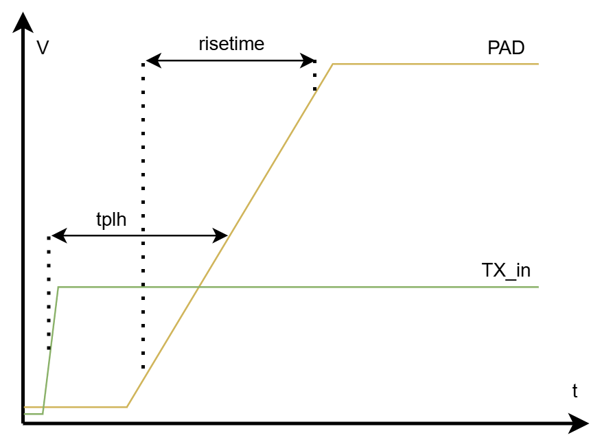
One of the most important transient characteristics of the driver is the rise and fall time, also called transition times. The rise time is defined as the time it takes for the pad voltage to go from 10% to 90% of the total voltage swing.
Contrary to VOH and VOL, the transition times are typically measured without any external DC bus current. However, the bus characteristics still have a huge influence on the rise and fall times! Depending on the bus capacitance, the rise and falltimes can vary an order of magnitude.
Typical values for the transition times differ greatly between systems. But as an example, a typical 10MHz GPIO can have transition times around 10ns, at a bus capacitance of 50pF.
It is important that the rise and fall times are fast enough for the chosen switching frequency. Otherwise, the pad might not complete its transition before the next bit is transmitted.
On the other hand, a too fast transition time can also cause issues as well. Faster rise and fall times have higher frequency components, which are more easily emitted over a wire. This could lead to EMC issues in the full system, especially with longer wire lengths. Additionally, rapid transitions can result in overshoot on the bus, particularly in systems prone to ringing behavior.
To address these concerns, slew rate compensation circuitry can be implemented to slow down the transition time, especially when there is minimal bus capacitance in the system.
Driver delay
The driver of course has some delay from its input to its output. It is measured from 50% of TX_in to 50% of the pad voltage.
Typically, this delay consists of a fixed delay due to the pre-driver, and a delay depending on the system due to a variable rise and fall time. As stated earlier, the rise and fall times can vary a lot from system to system because of varying capacitive bus load.
A subtlety to note is that the low-to high and high-to-low transition can have different delays. In some application, it is important that this delay difference is low enough.
One example where the delays have to be symmetrical is if the duty cycle of the pad is important. A concrete example: we have a 10MHz signal with a duty cycle of 50%. The pad is high for 50ns and then low for 50ns. If the delay difference is 10ns (tplh = 11ns, tphl = 1ns), the pad will be high for only 40ns and low for 60ns, resulting in a distorted duty cycle of 60%.
Pull resistance
While not directly tied to the driver design, pull resistance is related to pad control and is thus discussed here.
What happens to the bus voltage if not a single driver is controlling it directly? It will be dictated by parasitic leakage paths. The off resistance of the different drivers connected to the bus will determine if it is high or low. Or more plausible and even worse: the pad voltage will be somewhere mid-rail. This can cause a lot of issues in the system, for example a high supply current in the different receiver circuits.
But we don’t want to define the pad voltage! Because if a driver wants to use the bus for communication, it should still be able to control the pad voltage as it wants. So how do we solve this?
The answer is to control the pad through a medium-resistive path. When the pad is in high impedance (high-Z) mode, connecting it to a supply voltage via a resistor ensures a default state. A typical value for this resistance is 100kΩ. Connecting it to VSS is called a pulldown, while connecting it to VIO is called a pullup.
This approach allows drivers to overwrite the pad voltage for communication while maintaining control over the bus’s default state.
Receiver specifications
VIH and VIL
The receiver’s role is to interpret the pad’s electrical state (high or low) and translate it into a binary signal (0 or 1) sent to the chip’s core. This receiver output bit is called RX_out, or with some vendors C.
But what does a high and low pad state actually mean? This is defined via the specs VIH and VIL . If the pad voltage is above VIH, the receiver has to output a 1 to the core. Similarly, if the pad voltage is below VIL, the receiver outputs a 0. Typical values for VIH and VIL are 30% VIO and 70% VIO.
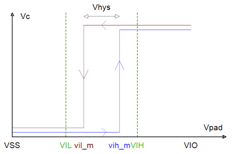
In above figure, vil_m and vih_m are the actual switchpoints of the measured receiver. These should at all times be in between the specified VIL and VIH.
Hysteresis
A second important specification of the receiver is hysteresis. In a receiver design, we make sure the point where the receiver goes from a 0 to a 1 (vih_m) is higher than the point where the receiver goes from a 1 to a 0 (vil_m). The difference between these two switch points is the amount of hysteresis.

A purpose of hysteresis is to mitigate the effects of noise.The pad is connected to a bus wire, and this bus can pick up high frequency noise. This means the pad signal is not a clean voltage, but rather the wanted signal with some noise on top of it. If the receiver would not have hysteresis (switchpoint up and down are equal), what would happen if the wanted signal is equal to the switchpoint? The pad voltage would very quickly go above and below the switchpoint, leading to RX_out switching erratically. This erratic switching could lead to issues in the logic down the line.
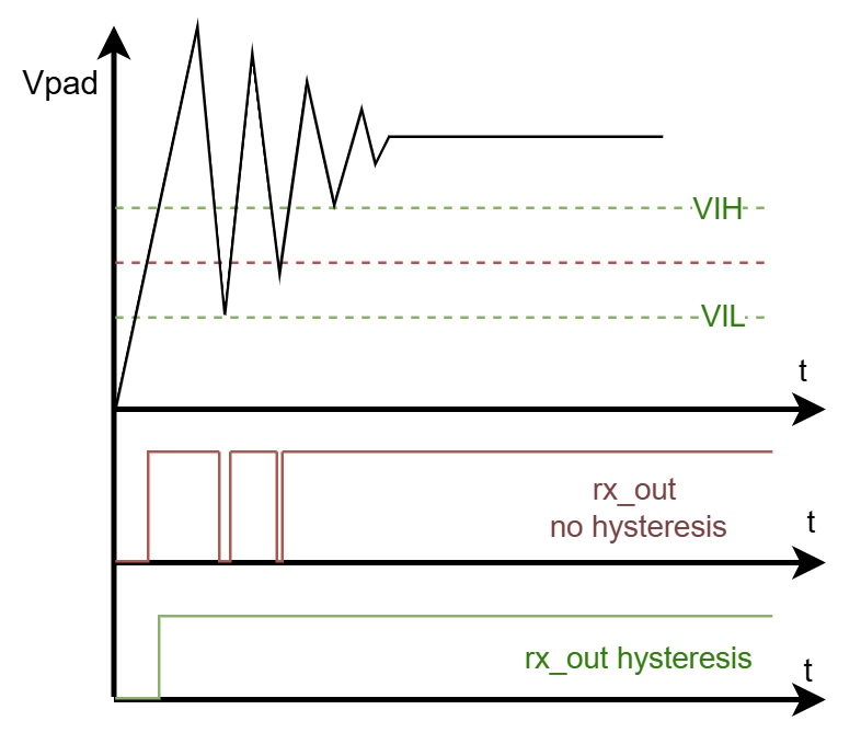
A second possible issue is a bus pulse with ringing. This is a common voltage waveform encountered on bus lines interconnecting systems, especially if the bus is of significant length. Again, we can see the receiver without hysteresis experiencing some short glitches on the output, while the version with hysteresis has a clean output
Introducing hysteresis resolves these issues. The amount of hysteresis required is depending on the amount of noise that is expected in the system. A Typical value is 5% to 10%.
More hysteresis is almost always better, although there is an upper limit due to VIH and VIL – the hysteresis curve has to fall in between VIH and VIL.
VIL, VIH and Vhys are often expressed as a percentage of VIO rather than an absolute voltage, although this is not strictly required.
Receiver delay
Lastly, the receiver has a certain propagation delay. This delay can be different for pad rising and pad falling. They are called tplh & tphl: propagation delay low to high & propagation delay high to low.
There are two ways to define this delay.
The first definition is the time difference between the moment the pad reaches 50%, to the moment RX_out reaches 50%. This definition is the most common due to its simplicity and ease of measurement.
The second definition is the time difference between the moment the pad reaches VIH/VIL (falling/rising pad), and the moment RX_out reaches 50%. This definition is a bit more complex, although more accurate to what is actually happening in the circuit. This measurement makes the delay independent of the risetime of the PAD.

Similar as in the driver, the low-to high and high-to-low transition can have different delays. For some applications, it can be important this difference stays low.
General specifications
Lastly, we have some specs not only related to the driver or receiver, but rather the complete circuit.
Current consumption
An important parameter for a lot of systems is the amount of current consumed by the GPIO. There are a lot of possible current specs, all depending on what state the I/O circuit is. Secondly, it is important to have an idea of the average current consumption as well as the peak currents consumed.
Some examples of interesting supply currents are: during isolation, during normal operation (not transmitting), normal operation (transmitting @ certain frequency), during sleep mode…
Pad impedance
Connecting a GPIO to the bus is not without impact. How big this impact is, is defined in the pad impedance spec.
First of all, we have the input impedance. This is equivalent to the leakage of the pad. Of course, if there is a pull resistance present, this dominates the pad impedance. Typical value is less than 10uA at rail voltages, when the pull is disabled.
Secondly, the pad also has an influence on the transient behavior of the bus. This is mainly defined by a bus capacitance. Typical value is a couple of pF.

3 responses to “I/O specs explained”
[…] Hysteresis: in order to filter out input noise or ringing […]
LikeLike
[…] background on the I/O circuits is available in a set of articles (I/O specs explained, Types of overvoltage tolerant I/O, Typical SOA violations in a stacked driver, […]
LikeLike
[…] I/O specs explained […]
LikeLike