
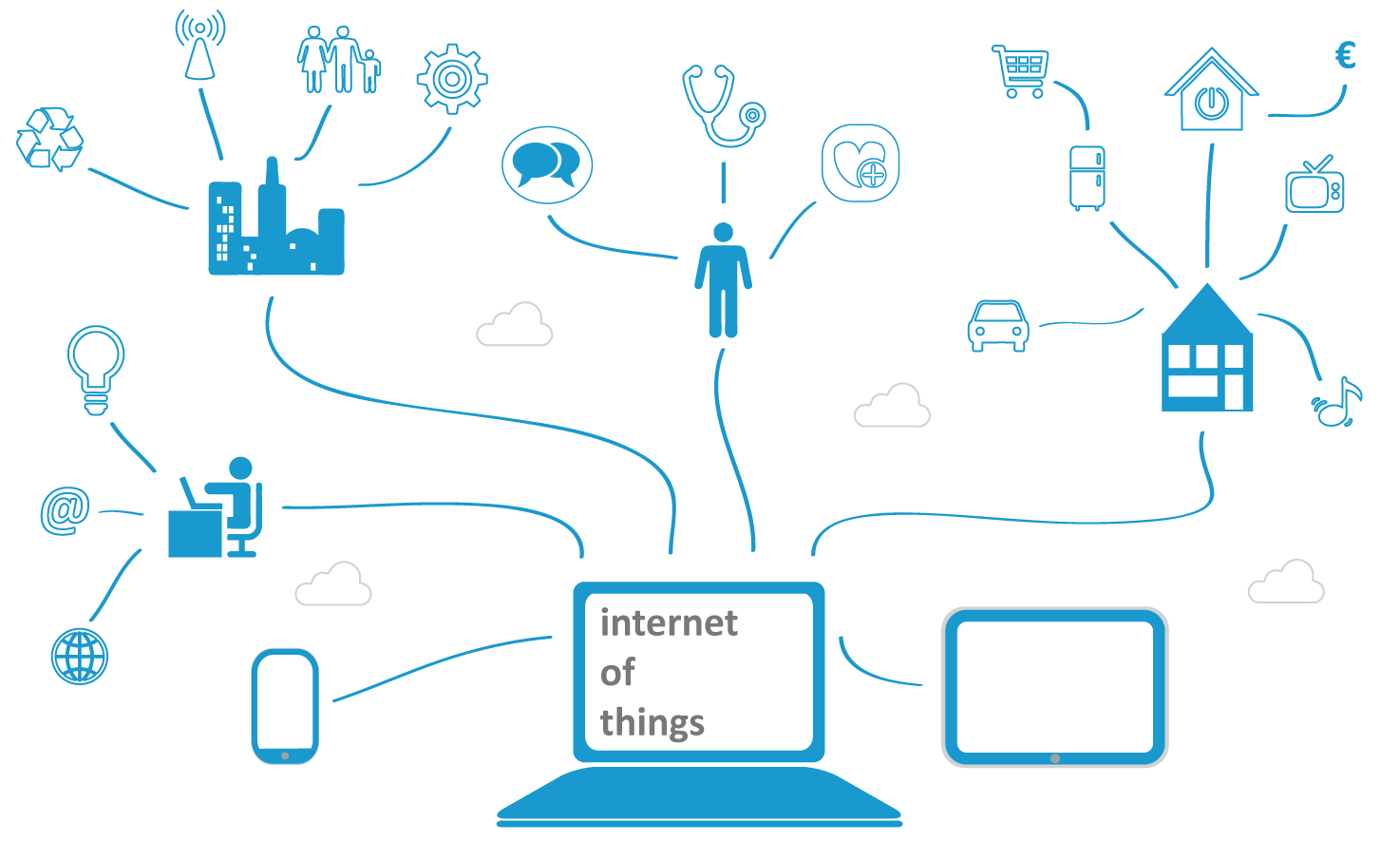
Internet of Things (IoT): Some call it a hype and wonder how connecting your refrigerator to internet will benefit anyone. But IoT is about much more than automated shopping lists. When you combine sensors, actuators, and networked intelligence the possibilities are endless. It can boost productivity, save resources and even prevent health issues.
The common denominator of these applications is that they all require one or more semiconductor chips. This explains why almost all semiconductor companies now suddenly have IoT related products. They focus on several aspects:
- Ultra low power electronics
- Connectivity
- Sensor integration
- Security
- Low cost
Many of the IoT chips can be made in older, depreciated fabrication plants (0.25um, 180nm, 130nm) that were top-notch 20 years ago. One would argue that foundries have covered every aspect of Electrostatic Discharge (ESD), Electrical Overstress (EOS) and Latch-up in these old processes long ago. However, what we have learned by supporting innovative semiconductor startups is that many of the applications in IoT (Internet of Things) require non-standard on-chip ESD protection clamps for a number of reasons.
1. Non-standard signal voltage
Several IoT systems include sensor or actuator interfaces that have distinctive signal conditions. Some actuators need a much higher driving voltage (5V or even 20V), beyond the typical I/O interfaces provided by the foundry or I/O providers. Similarly, small signals (order of a few mV or mA) captured by sensors for motion detection and touch remain hidden in the noise or are lost due to leakage created by General Purpose Input Output circuits (GPIO).
2. Low leakage requirement
There is another reason why designers worry about the leakage of the ESD protection clamps provided by the foundry. A lot of the IoT applications are running on a small battery or harvest energy from the surrounding. Designers move heaven and earth to reduce the leakage of the functional circuits. Foundries on their end provide special ‘ULP’ process options to reduce both standby and dynamic power. It would be unwise to nullify all that work through the use of leaky ESD protection clamps integrated in the standard IO circuits.
3. Sub-systems are powered down
To reduce the leakage only a small part of the system is awake all the time. All the other circuits are turned off most of the time. The entire system is only running when there is new data available. Traditional ESD protection could again ruin the efforts because signals applied on the I/O’s can power-up a functional block that is not required at that time. Moreover, conventional ESD protection based on slew rate detection are triggered every time the domain is restarted.
4. Wireless interfaces
Every (innovative) system needs to communicate with its surroundings or directly with the internet. Therefore wireless interfaces and/or high speed digital connections can be found on almost all of the IoT systems. For both (wireless, wired) the IC designer needs on-chip ESD protection with low parasitic capacitance (200fF or lower). This means that the general purpose interface circuits provided by the foundry are not suitable and alternatives have to be created.
5. System level protection, on the chip
A lot of the innovative systems are meant to be low-cost and mobile and also this relates to ESD in several ways. To reduce the size of the system and the Bill of Materials (BOM), system designers are removing board level ESD protection blocks from the mini-Printed Circuit Boards (PCB). 20 years ago, such Transient Voltage Suppressors (TVS) devices were added on PCBs to protect ICs against ESD stress during the actual use of products. Without such TVS protection and due to the much shorter PCB traces Integrated Circuits are stressed with more severe ESD stress like IEC 61000-4-2. This has a factor of 4 to 5 higher stress current compared to component level Human Body Model (HBM) ESD.
Moreover, the probability of ESD-stress is much higher in those mobile systems as they are operated in so-called harsh environments. Consider that plastic (e.g. smartphone cover) rubbed by cloth (your back-pocket) generates a lot of charges – just millimeters away from the high speed USB port.
Conclusion
Clearly, IC designers need to think about the ESD protection strategy for their IoT system.
More information?
- Get more details in our White Paper [Link] on ESD protection for Internet of Things applications.
- Sofics engineers have supported several RF projects for IoT in the past. In this 2010 publication we described the ESD protection approach for indoor positioning and Bluetooth, GPS wireless applications [Link]. At that time our customer was using TSMC 90nm and 40nm CMOS technology
- Contact us if you like to know how the Sofics approach benefits your IoT application.